Top Page > News Release
2017/5/22
Sony’s F65 CineAlta Camera, which APi collaborated in the optical data transmission technology, was honored Academy’s Scientific and Engineering Awards.
Link-1 Link-2
Sony’s F65 CineAlta Camera, which APi collaborated in the optical data transmission technology, was honored Academy’s Scientific and Engineering Awards.
Link-1 Link-2
2017/4/21
In the technical private show held by KT Group during 19th to 20th April, APi demonstrated a tiny high-resolution POF camera co-developed with KT Group and Honda Tsushin Kogyo Co., Ltd.
Link-1 Link-2(5/22 added)
POF: Plastic Optical Fiber
In the technical private show held by KT Group during 19th to 20th April, APi demonstrated a tiny high-resolution POF camera co-developed with KT Group and Honda Tsushin Kogyo Co., Ltd.
Link-1 Link-2(5/22 added)
POF: Plastic Optical Fiber
2016/2/8
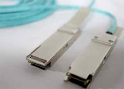
APi has released 100 Gbps Infiniband EDR QFSP+ AOC.
For more information, click here. (PDF file)
APi has released 100 Gbps Infiniband EDR QFSP+ AOC.
For more information, click here. (PDF file)
 2015/11/11
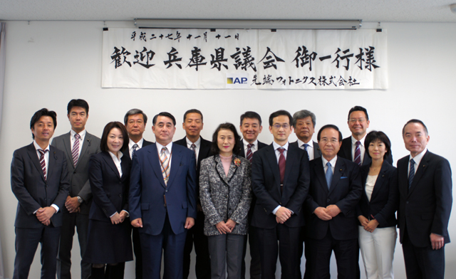
The Hyogo Prefectural Assembly Standing Committees on Idustrial Workers Affairs paid visit to APi as part of the committees' research study concerning industry-academia-government cooperation.
2015/8/27~28
Exhibitor at the "Innovation.Japan 2015". APi will be exhibiting our products and technologies at the "Innovation.Japan 2015" in Tokyo, in the Big Site convention facilities.
http://www.jst.go.jp/tt/fair/
Exhibitor at the "Innovation.Japan 2015". APi will be exhibiting our products and technologies at the "Innovation.Japan 2015" in Tokyo, in the Big Site convention facilities.
http://www.jst.go.jp/tt/fair/
 2015/6/5
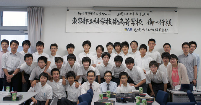
Students and teachers of the Tokyo Metropolitan High School of Science and Technology paid visit to APi as part of its students carreer design tour experience.
2014/11/19~11/21
Exhibitor at the "New Value Creation Exhibition 2014". APi will be exhibiting our products and technologies at the "New Value Creation Exhibition 2014" in Tokyo, in the Big Site convention facilities. This is to be held in November, for three days (19th to the 21st).Please come visit our booth situated near the entrance 'East Hall 2・3'
http://shinkachi.smrj.go.jp/
2014/11/11~14
APi senior management gave presentations in ACP 2014 (Asia Communication Photonics Conference) held in Shanghai.
・Invited talk by APi's Chief Technology Advisor and Board Member Prof. Yoshiaki Nakano
・Workshop 8 : "Optical Interconnect - from devices to system application"
Session chair: APi's Technical Advisor Dr.Takashi Mikawa, Speakers: APi's Technical Advisor Dr.Ueda Osamu (Prof. at Kanazawa Institute of Technology) APi's VP and Board Member Dr. Foo Cheong, YIT Please refer here for details.
http://www.acp-conf.org/
2014/4/24
On April 24th, 2014, APi was given coverage in the Nikkei Business Daily (The Nikkei Sangyo Shimbun, a cutting-edge industry newspaper issued by Japan most influencial publishing group).
For details, please refer to here (pdf file)
On April 24th, 2014, APi was given coverage in the Nikkei Business Daily (The Nikkei Sangyo Shimbun, a cutting-edge industry newspaper issued by Japan most influencial publishing group).
For details, please refer to here (pdf file)
2013/9/12
On Sept. 12th, 2013, APi was given first-page top coverage in Nikkan Kogyo Shimbun (a well established leading business & technology daily newspaper in Japanese language) for article titiled "100 Gigabit per second Optical Fiber Cable for Communication shows bright prospects for practical implementation".
For details, please refer to here (pdf file)
2013/3/30
On Mar. 30th, 2013, APi was covered in the evening edition of Nihon Keizai Shimbun (a leading daily newspaper on economic and financial matters with large worldwide circulation, issued by Japan most influencial publishing group).
For details, please refer to here (pdf file)
On Mar. 30th, 2013, APi was covered in the evening edition of Nihon Keizai Shimbun (a leading daily newspaper on economic and financial matters with large worldwide circulation, issued by Japan most influencial publishing group).
For details, please refer to here (pdf file)
 2013/4/10~12
Exhibitor at the "Photonix2013". APi will be exhibiting our products and technologies at the "Photonix2013" in Tokyo, in the Big Site convention facilities.
http://www.photonix-expo.jp/
 2013/1/11
APi was covered by TV media in "News Answer" of TV Tokyo Corp. as part of a report concerning the "Abe-nomics" (A coined phrase fused from 'Prime Minister Shinzo Abe' and 'economics' to mean the economic revive plan pioneering by Prime Minister Abe leadership). APi's Chief Technology Officer (CTO), Dr.Song made appearance in the interview.
2012/2/22
 APi is pleased to announce a new product, an Active Optical Cable for use in InfiniBand interconnections, which has passed IBTA (InfiniBand Trade Association) authorization. These cables allow for bi-directional serial links between processors and/or peripherals for high-speed data flow.
・Type DDR:20Gbps 1~100m
・Type QDR:40Gbps 1~100m
Interested parties please click here for further details (PDF File). <Reference> We are listed as one of the IBTA Integrators on the homepage of the Authorization company(IBTA Integrators List).
http://www.infinibandta.org/content/pages.php?pg=integrators_list_overview
APi is pleased to announce a new product, an Active Optical Cable for use in InfiniBand interconnections, which has passed IBTA (InfiniBand Trade Association) authorization. These cables allow for bi-directional serial links between processors and/or peripherals for high-speed data flow.・Type DDR:20Gbps 1~100m
・Type QDR:40Gbps 1~100m
Interested parties please click here for further details (PDF File). <Reference> We are listed as one of the IBTA Integrators on the homepage of the Authorization company(IBTA Integrators List).
http://www.infinibandta.org/content/pages.php?pg=integrators_list_overview
 2011/6/1~3
We will have an exhibit at the “JPCA show 2011” at which we will be presenting our latest products. This will take place in June over three days (1st to the 3rd) in the Tokyo International Exhibition Center better known as the Tokyo Big Sight and is sponsored by the Japan Electronics Packaging and Circuits Association.
http://www.jpcashow.com/show2011/English/
 2011/4/13~15
We have been accepted to present at “Photonix2011” which will be held on the 13th to 15th of April 2011 at the Big Site Tokyo, we will be exhibiting our products.
http://www.photonix-expo.jp/photonix/en/
2010/08/16
Reported on the front page of the Nikkei Business Daily Newspaper
"300 Gigabit inter LSI chip communication, even through curved interconnects"
For further details, click here(PDF File)
Reported on the front page of the Nikkei Business Daily Newspaper
"300 Gigabit inter LSI chip communication, even through curved interconnects"
For further details, click here(PDF File)
2010/7/7~9
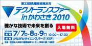 We will have an exhibit at the “Technology Fair in Kawasaki 2010” at which we will be presenting our latest products.
This will take place in July over three days (7th to the 9th) in the Kanagawa Science Park (KSP) Innovation Centre and is sponsored by the Kanagawa Industrial Promotion Center.
We will have an exhibit at the “Technology Fair in Kawasaki 2010” at which we will be presenting our latest products.
This will take place in July over three days (7th to the 9th) in the Kanagawa Science Park (KSP) Innovation Centre and is sponsored by the Kanagawa Industrial Promotion Center.
http://www.tech-kawasaki.jp/ttk2010/
We will have an exhibit at the “Technology Fair in Kawasaki 2010” at which we will be presenting our latest products.
This will take place in July over three days (7th to the 9th) in the Kanagawa Science Park (KSP) Innovation Centre and is sponsored by the Kanagawa Industrial Promotion Center. http://www.tech-kawasaki.jp/ttk2010/
2010/6/18
We will be giving a presentation at the Agilent Symposium Series 2010 which will be held on the 17th and 18th of June. The title of the talk will be “(Mixing electronics and optics) the development of mixed PCB’s using ecological and open innovation techniques”. This symposium will take place at the Hachioji offices of Agilent Technologies in Japan and our talk will be on the 18th of June.
http://www.agilent.co.jp/find/sympo
2010/6/2~4
 We will have an exhibit at the “JPCA show 2010” at which we will be presenting our latest products. This will take place in June over three days (2nd to the 4th) in the Tokyo International Exhibition Center better known as the Tokyo Big Sight and is sponsored by the Japan Electronics Packaging and Circuits Association.
http://www.jpcashow.com/show2010/English/index.html
We will have an exhibit at the “JPCA show 2010” at which we will be presenting our latest products. This will take place in June over three days (2nd to the 4th) in the Tokyo International Exhibition Center better known as the Tokyo Big Sight and is sponsored by the Japan Electronics Packaging and Circuits Association. http://www.jpcashow.com/show2010/English/index.html
2010/01/20~22
 We have been accepted to present at “FOE2010”
At this show, “The Fiber Optics Exposition 2010”, which will be held on the 20th to 22nd of January 2010 at the Big Site Tokyo, we will be exhibiting our products.
We have been accepted to present at “FOE2010”
At this show, “The Fiber Optics Exposition 2010”, which will be held on the 20th to 22nd of January 2010 at the Big Site Tokyo, we will be exhibiting our products.
http://www.foe.jp/foe/
We have been accepted to present at “FOE2010”
At this show, “The Fiber Optics Exposition 2010”, which will be held on the 20th to 22nd of January 2010 at the Big Site Tokyo, we will be exhibiting our products. http://www.foe.jp/foe/
At the aforementioned show we shall also be giving a talk in the related expert skills seminar, which takes place during the exhibition. The title of our talk is “Open innovation strategy for the introduction of optical interconnects into PCB boards.
Date: Friday 22nd of January 2010 at 9:30-12:00 Session: FOE-11
http://www.foe.jp/jp/conference10/foe.phtml#FOE11
Date: Friday 22nd of January 2010 at 9:30-12:00 Session: FOE-11
http://www.foe.jp/jp/conference10/foe.phtml#FOE11
2009/12/10~12
 We have been accepted to present at the “SMFG Environment-Related Business Forum”
At this show, “SMFG Environment-Related Business Forum held within Eco-Products 2009”, which will be held on the 10th to 12nd of December 2009 at the Big Site Tokyo, we will be exhibiting our products.
We have been accepted to present at the “SMFG Environment-Related Business Forum”
At this show, “SMFG Environment-Related Business Forum held within Eco-Products 2009”, which will be held on the 10th to 12nd of December 2009 at the Big Site Tokyo, we will be exhibiting our products.
http://eco-pro.com/eco2009/
We have been accepted to present at the “SMFG Environment-Related Business Forum”
At this show, “SMFG Environment-Related Business Forum held within Eco-Products 2009”, which will be held on the 10th to 12nd of December 2009 at the Big Site Tokyo, we will be exhibiting our products. http://eco-pro.com/eco2009/
2009/8/7
Inclusion in the “First ‘monotsukuri’ skilled manufacture product development business support of 2009 This is a program to support and aid businesses in the issues of manufacturing and selling of products and is overseen by the National Federation of Small Business Associations here in Japan.
http://www.chuokai.or.jp/josei/info_m_090807s.html
2009/06/03
Our company was taken up by Nihon Keizai Shinbun (Japan economic newspaper) in its morning edition of Jun 3, 2009 issue.
Our company was taken up by Nihon Keizai Shinbun (Japan economic newspaper) in its morning edition of Jun 3, 2009 issue.
For details, please refer to here(pdf file).
2008/12/02
The subject of the speech: “ The wait is over. New market for optical interconnection is going to take-off. Open Innovation Strategy is the key for development acceleration”.
The subject of the speech: “ The wait is over. New market for optical interconnection is going to take-off. Open Innovation Strategy is the key for development acceleration”.
For details, please refer to here(pdf file).
2008/09/30
Advantest Corp has developed a new optical PCB technology.
Advantest Corp has developed a new optical PCB technology.
Advantest has developed an optical PCB technology that enables signal transmission at 160 Gbps (G means one billion) in collaboration with Advanced Photonics, Inc. ( head office in Ota-ku, Tokyo).
For details, please refer to here(pdf file).
2008/09/12
The Kahoku Simpo, an influential newspaper in North-Eastern part of Japan, covered in its 12 September 2008 issue the new optical PCB technology which we developed in collaboration with Advantest Corporation, a leading semiconductor testing equipment manufacturer.
The Kahoku Simpo, an influential newspaper in North-Eastern part of Japan, covered in its 12 September 2008 issue the new optical PCB technology which we developed in collaboration with Advantest Corporation, a leading semiconductor testing equipment manufacturer.
For details, please refer to here(pdf file).
2008/09/10
The talk in the session titled “ The new market accelerated by open innovation : Optical Interconnection” was welcomed by unexpectedly large number of audience and achieved big success.
The talk in the session titled “ The new market accelerated by open innovation : Optical Interconnection” was welcomed by unexpectedly large number of audience and achieved big success.
We would like to express our thanks to all of the people who attended the seminar.
Excerpt from the handouts distributed in the seminar is here(pdf file).
2008/07/11
We have decided to join "Inter Opt 08".
We have decided to join "Inter Opt 08".
Our products will be exhibited in Inter Opt 08 which is to be heldin Makuhari Messe from 10 September through 12 September this year.
http://www.oitda.or.jp/main/io/io08home.html
2008/06/17
2008/06/03 Nikkei Business Daily covered our company.
2008/06/03 Nikkei Business Daily covered our company.
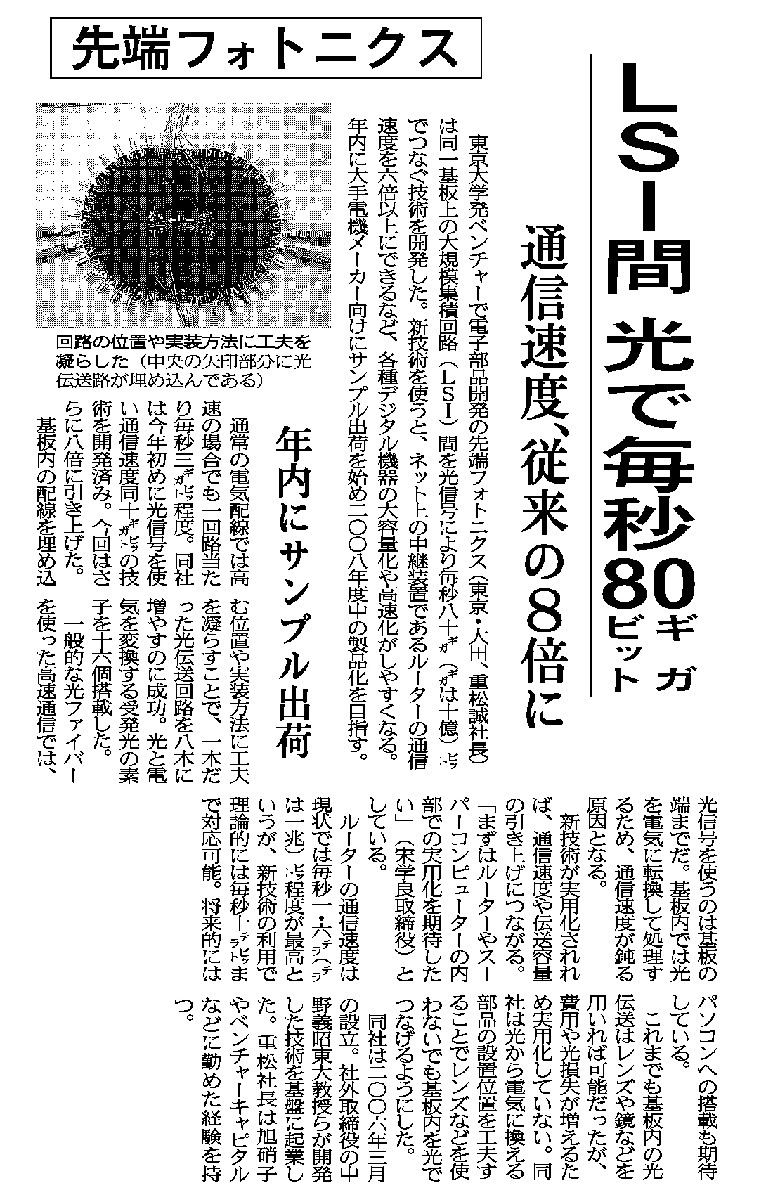
Advance Photonics has succeeded in optically interconnecting LSIs in a router placed 30 Centimeters apart.
Advanced Photonics, Inc.(APi) , a venture company spun out from the University of Tokyo ( Ota-ku, Tokyo, President: Mr.Makoto Shigematsu) has succeeded in developing technology to optically interconnect large scale integrated circuits(LSI) in a router which regulates traffic of large volume data communications.
This technology allows faster signal transmission between LSIs than the conventional electric interconnection, and the volume of data that can be handled by one router can be increased six fold from the current level.
The interconnection of LSIs placed 30 Centimeters apart was successfully achieved by embedded interconnection.
The technology that APi has successfully developed optically interconnects LSIs on PCB incorporated in a router.
There are eight optical interconnection channels made of a kind of epoxy resin which has higher refractive index, embedded on PCB made of another kind of epoxy resin. Its length is 30 Centimeters, and both width and height are 50 μm( μ denotes one- millionth) .
At one end of the optical interconnection, a semiconductor laser which converts electric signal to photo signal is attached, and at the other end, there is a photo acceptance unit to reconvert the photo signal to electric signal.
In the test run, one optical interconnection channel transmitted 10 Giga bits per second (Giga denotes billion) , making total transmission of 80 Giga bits by eight interconnection channels.
By last year, APi had succeeded in transmission for the length of 7 Centimeters , but this was not long enough for commercial use.
It has successfully extended the transmission distance to 30 Centimeters, which is compatible with commercial use, by reducing transmission loss of signal with enhanced dimensional accuracy of interconnection as well as enhanced positional accuracy of incoming and outgoing optical signal.
The maximum transmission capacity of the present electric interconnection is three Gbps while optical interconnection can achieve more than 10Gbps.
Furthermore, channels of interconnection for electric transmission must have certain distance between them due to the problem of mutual interference, but optical signal is free from such interference, thus allowing more numbers of channels set closer each other.
APi estimates that the router of the same size, if interconnected by light, can handle data six times more than electrically interconnected router.
Although technologies to make optical interconnection on the surface of PCB have been proposed, the embedded optical interconnection can benefit from more use of the surface , allowing more LSIs and other components to be mounted.
For further details, click here (PDF file)
2008/01/17
Our company was covered by Jan 17, 2008 issue of The Nikkan Kogyo Shimbun in its Electronic Devices Section.
Our company was covered by Jan 17, 2008 issue of The Nikkan Kogyo Shimbun in its Electronic Devices Section.
“Photo-Electric Integrated Circuit Board with 8 optical transmission lines”
Advanced Photonics, Inc. (Ota-ku, Tokyo, President Mr.Makoto Shigematsu, TEL:03-5452-5475) prototyped a photo-electric integrated circuit board with optical transmission lines increased from one to 8. The photo-electric integrated circuit board uses optical signal for communications among LSIs on the printed circuit board, which make transmission at the speed of 10 Giga-bit per second (Giga meaning one billion). It enables three times as high and fast transmission as electronic wiring.
The prototype this time has succeeded in achieving 80 Giga-bit transmission through optical transmission lines increased to 8. Advanced Phtonics displayed it in “Fiber Optics Expo” opened on 16th at Tokyo Big Site in Ariake, Tokyo.
For further details, click here (PDF file)
2007/11/19
Our company has decided to take part in “FOE2008”.
Our company has decided to take part in “FOE2008”.
We have decided to join this event next year as we won favorable recognition by our potential customers this year.
We plan to exhibit our new products in the 8th Fiber Optics Expo to be held in Tokyo Big Site from 16 to 18 of January 2008.http://www.foe.jp/foe/
2007/07/18
Nikkei Business Daily covered our company.
Nikkei Business Daily covered our company.
80Gbits per second optical transmission among LSIs- 8 times faster than conventional method .Advanced Photonics, Inc., a venture business company spun off the University of Tokyo and engaged in development of electronic parts, has succeeded in developing technology to connect Large Scale Integrated Circuits (LSI) placed on the board via optical signal at the speed of 80 Giga(meaning billion) bits per second.The application of the new technology will make it easier to realize higher capacity and higher speed, by more than six times, for various digital equipment, including router which is a relaying equipment on the net.
Under the conventional electric wiring, transmission speed is around three Gaga bit per second at its best. Advanced Photonics had developed technology early this year for 10 Giga bit transmission via optical signal and this time it increased the speed by 8 times.
They succeeded in increasing the number of optical transmission lines from one to eight by making use of innovative method in designing the place of embedding the wiring as well as its mounting. There are 16 photo emitting-accepting devices installed on the board which converts light and electricity.
In the conventional high speed communications through optical fiber, usage of light ends at the edge of the board. Once it reaches the board, light is converted to electricity for processing and this was one of the causes for communications speed tends to be decreased.
When put into practical use, the new technology will bring about higher communications speed and higher transmission capacity. “We may expect that it is first employed in routers and supercomputers” said Mr. Xueliang Song, director of Advanced Photonics.
At present, the maximum communication speed of routers is about 1.6 Tera (trillion) bits per second. Theoretically, the new technology allows 10 Tera bit transmission per second. It might be used in personal computers in the future.
Although optical transmission on the board was not impossible so far by using lens and mirror, the high cost and light loss associated with them have prevented the commercialization. Advanced Photonics has succeeded in optical interconnection on the board by creative methods in placing the devices which convert light to electricity.
Advanced Photonics was established in March 2006, based on the technology developed by Prof. Yoshiaki Nakano of the University of Tokyo , who is now an external board member of the company.
For further details, click here(PDF File)
2007/06/08
Prime Minister’s Award to Prof. Yoshiaki Nakano of Tokyo Univ., director and the supreme advisor to our company
Prime Minister’s Award to Prof. Yoshiaki Nakano of Tokyo Univ., director and the supreme advisor to our company
Prof. Yoahiaki Nakano won 2007 Prime Minister’s Award for his NEDO –related project theme of “Development of Photonic Network Technology (2002-2006)” in Citation for Industry-Academy-Government Collaboration. This award is given to individuals or organizations for their distinguished achievement in Industry-Academy-Government collaboration activities. It is expected that the award-winning technology make great contributions to creation of new industries and enhancement of global competitiveness of our nation.
http://www.nedo.go.jp/informations/press/190608_1/190608_1.html
2007/05/01
We have decided to join “Inter Opt 07”.
We have decided to join “Inter Opt 07”.
Our products will be exhibited in Inter Opt 07 which is to be held in Makuhari Messe from 11 July through 13 July this year.
http://www.oitda.or.jp/main/io/io07home-j.html
2007/03/20
Prof. Yoshiaki Nakano of Tokyo University, the supreme advisor to our company, won Ichimura Prize.
Prof. Yoshiaki Nakano of Tokyo University, the supreme advisor to our company, won Ichimura Prize.
Prof. Nakano was awarded Contribution Award of 39th Ichimura Science & Technology Prize for his “Development of Semiconductor Optical Device & Circuit for Digital Photonics”. This award is given to research engineers from universities and research institutions for their achievements which contribute to progress of academic studies and have potential to be put into practical use.
http://www.sgkz.or.jp/prize/science/39/index.html
2007/01/18
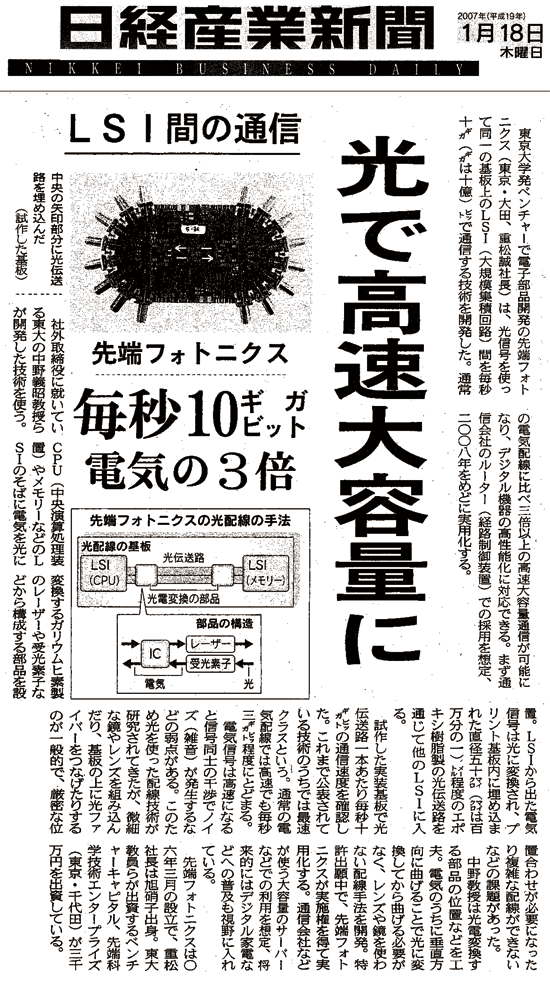
Our company was covered by Nikkei Business Daily in its top page on Jan 18,2007.
Our company was covered by Nikkei Business Daily in its top page on Jan 18,2007.
Transmission between LSIs , high-speed & high-capacity by light, 10 Giga bit per second, 3 times higher than electricity, developed by Advanced Photonics Advanced Photonics, Inc., a venture company spun off the University of Tokyo and engaged in development of electronic parts, has succeeded in developing technology to connect Large Scale Integrated Circuits (LSI) placed on the board via optical signal at the speed of 10 Giga(meaning billion) bits per second.The new technology will make it possible to realize higher- capacity and higher- speed by three times of the conventional electric wiring and bring about higher performance for various digital equipment. Advanced Photonics expects the first application in routers (routing equipment) for communications companies with commercialization targeted in 2008.
The basic technology was developed by Prof. Yoshiaki Nakano of the University of Tokyo who is an external director of the company.There are GsAs laser photo acceptance unit which converts electricity to light placed near LSIs of CPU (Central Processing Unit) and memory.Electric signal coming out of an LSI goes through optical transmission line, embedded in printed circuit board, of about 50 micron( micron means one millionth) meter in diameter made of epoxy resin, and enters into another LSI.
According to the company, the prototype board achieved transmission speed of 10 Giga bit per second, claiming the top class speed thus far reported. The conventional electric wiring transmits no more than 3 Giga bits per second at its best.
Electric signal transmission has its weakness in that it causes noise when electric signals are exchanged at very high speed. For this reason, wiring technology to use light has been studied but it had its own problems. The conventional technology incorporates minute mirror or lens, and connects optical fibers on the board, thus requiring precision alignment, and complicated wiring was not feasible.
Prof. Nakano made the use of various creative methods including the location of the parts for photoelectric conversion, and succeeded in developing a method where direction of signal is vertically bent while it is still in electricity, thus eliminating the need to bend it after converted into light, which in turn makes it unnecessary to use lens nor mirror.He has already applied patent for it and Advanced Photonics got the license to commercialize the technology.
It expects application in high-capacity servers used in communications companies to begin with, and in the future application may expand to digital household appliances.
2006/12/01
We have decided to join “FOE2007”.
We have decided to join “FOE2007”.
It was decided that our products will be displayed in the booth of TOUDAI TLO, Ltd., the licensing arm of the University of Tokyo, in the next year’s 7th Fiber Optics EXPO to be held in Tokyo Big Site from 24 through 26 January.
http://www.foe.jp/foe/
2006/10/03
Our company’s project was selected as eligible for subsidy by New Energy and Industrial Technology Development Organization (NEDO) in its Fiscal 2006 Second “University-oriented Business Creation- Commercialization Research & Development Projects”.
Our company’s project was selected as eligible for subsidy by New Energy and Industrial Technology Development Organization (NEDO) in its Fiscal 2006 Second “University-oriented Business Creation- Commercialization Research & Development Projects”.
NEDO accepted application for subsidies from May 1 through July 12, 2006 under its Fiscal 2006 Second “University-oriented Business Creation- Commercialization Research & Development Projects. A total of 56 applications were made and NEDO selected 32 projects for subsidies through its Review Board consisted of people of experience or academic standing, who reviewed the proposed projects and made evaluation in detail.
Our company’s project, “High-speed, high-capacity optical wiring board commercialization research & development” is among the selected projects. The NEDO project subsidies aim at matching corporate needs and seeds held by universities for joint research & development by Industry-Academy Collaboration. The subsidized projects are expected to be put into commercialization within two years after the joint research & developments are completed.
http://www.nedo.go.jp/informations/koubo/181003_2/181003_2.html
2006/09/01
We moved our registered head office.
We moved our registered head office.
New head office address: 7-1-103 Haneda Asahicho, Ota-ku, Tokyo
http://www.pio-ota.jp/facility/bic.html
2006/03/15
Advanced Photinics, Inc. was incorporated.
Advanced Photinics, Inc. was incorporated.
Registered head office address: 6-2, Marunouchi 2-chome, Chiyoda-ku, Tokyo